|


|
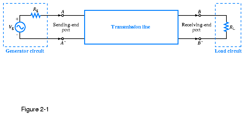
Figure 2.1: | A
transmission line is a two-port network connecting a generator circuit
at the sending end to a load at the receiving end.
|
|
|
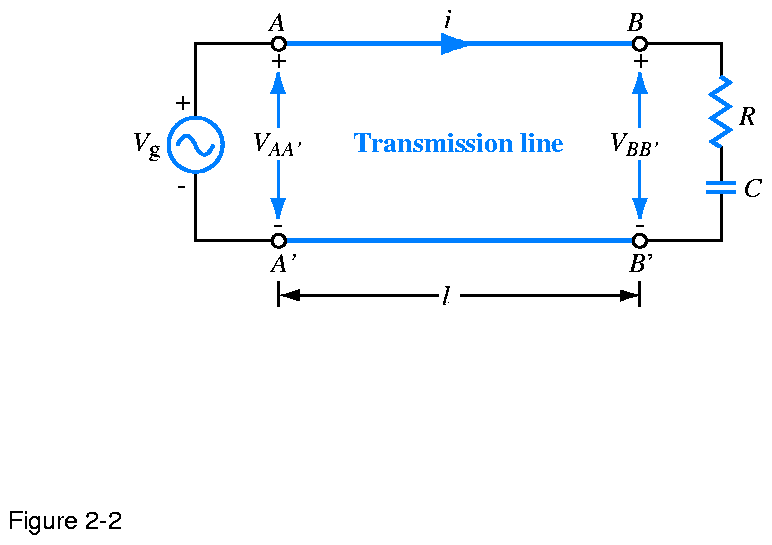
Figure 2.2: | Generator connected to an RC circuit through a
transmission line of length l.
|
|
|
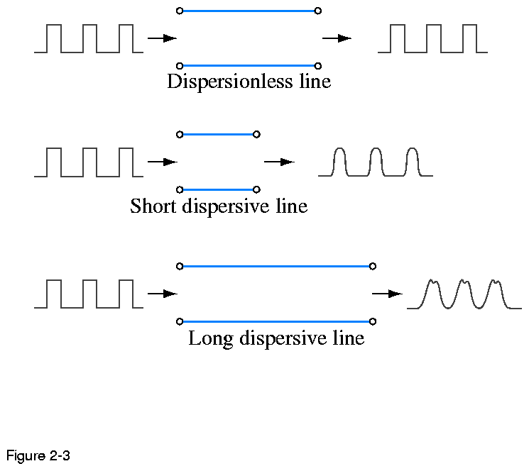
Figure 2.3: |
A dispersionless lines does not distort signals passing
through it regardless of its length, whereas a dispersive line distorts
the shape of the input pulses because the different frequency
components propagate at different velocities. The degree of
distortion is proportional to the length of the dispersive line.
|
|
|
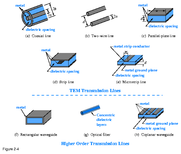
Figure 2.4: | A few examples of transverse electromagnetic (TEM) and
higher-order transmission lines.
|
|
|
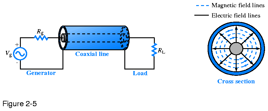
Figure 2.5: | In a coaxial line, the electric field lines are in the
radial direction between the inner and outer conductors, and the
magnetic field forms circles around the inner conductor.
|
|
|
Figure 2.6: |
Regardless of its actual shape, a TEM transmission line
is represented by the parallel-wire configuration shown in (a). To
analyze the voltage and current relations, the line is subdivided into
small differential sections (b), each of which is then represented by
an equivalent circuit (c).
|
|
|
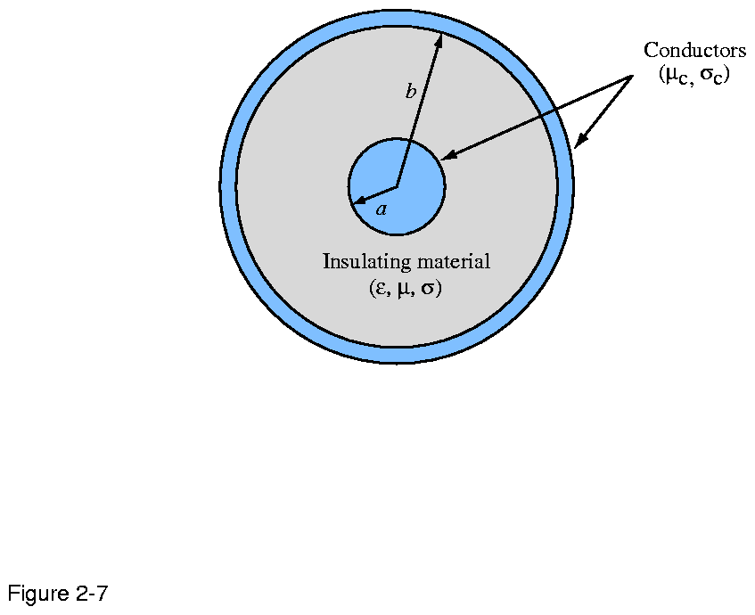
Figure 2.7: |
Cross section of a coaxial line with inner conductor of
radius a and outer conductor or radius b. The conductors
have magnetic permeability  c,
and conductivity c,
and conductivity  c, and
the spacing material between the conductors has permittivity c, and
the spacing material between the conductors has permittivity
 , permeability
, and conductivity . , permeability
, and conductivity .
|
|
|
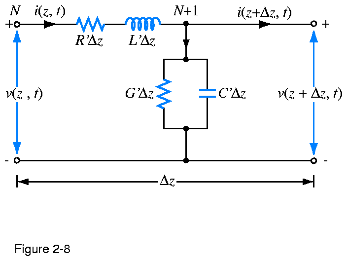
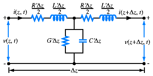
Figure 2.8: |
Equivalent circuit of a differential length  z of
two-conductor transmission line. z of
two-conductor transmission line.
|
|
|
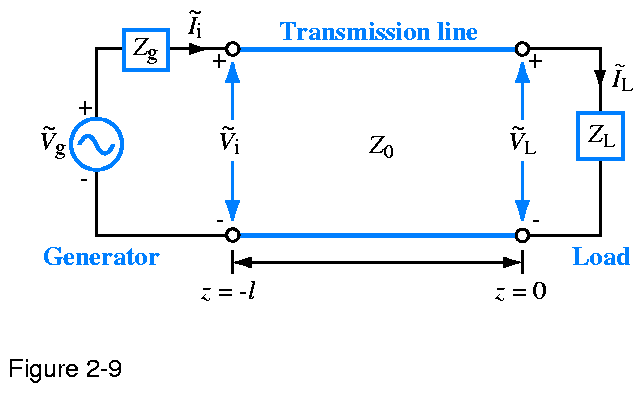
Figure 2.9: |
Transmission line of length l connected on one end
to a generator circuit and on the other end to a load ZL. The load
is located at z=0 and the generator terminals are at z=l.
|
|
|
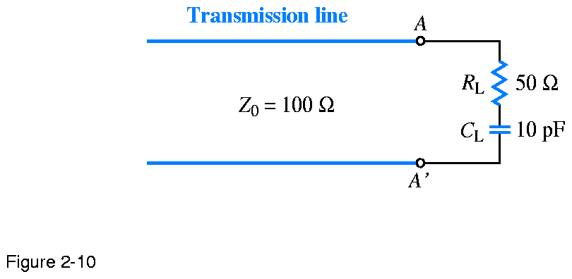
Figure 2.10: | RC load (Example 2-2).
|
|
|
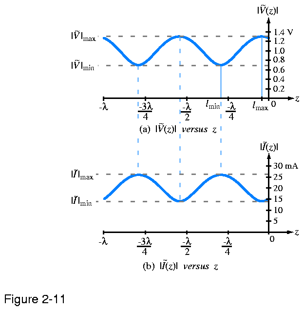
Figure
2.11: |
Standing-wave pattern for (a) |V(z)| and
(b) |I(z)| for a lossless transmission line of
characteristic impedance Z0=50  , terminated in a load with a
reflection coefficient , terminated in a load with a
reflection coefficient  =0.3ej30o. The magnitue of the
incident wave |V0+| = 1 V. The standing-wave
ratio is S = |V|max/|V|min= 1.3/0.7 = 1.86. =0.3ej30o. The magnitue of the
incident wave |V0+| = 1 V. The standing-wave
ratio is S = |V|max/|V|min= 1.3/0.7 = 1.86.
|
|
|
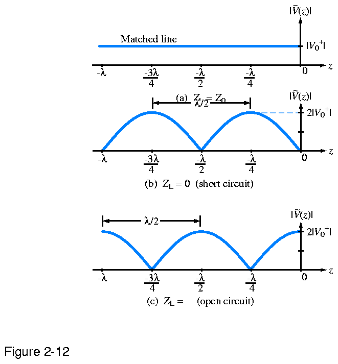
Figure
2.12: |
Voltage standing-wave patterns for (a) a matched load,
(b) a short-circuited line, and (c) an open-circuited line.
|
|
|
Figure 2.13: | Slotted coaxial line (Example 2-5).
|
|
|
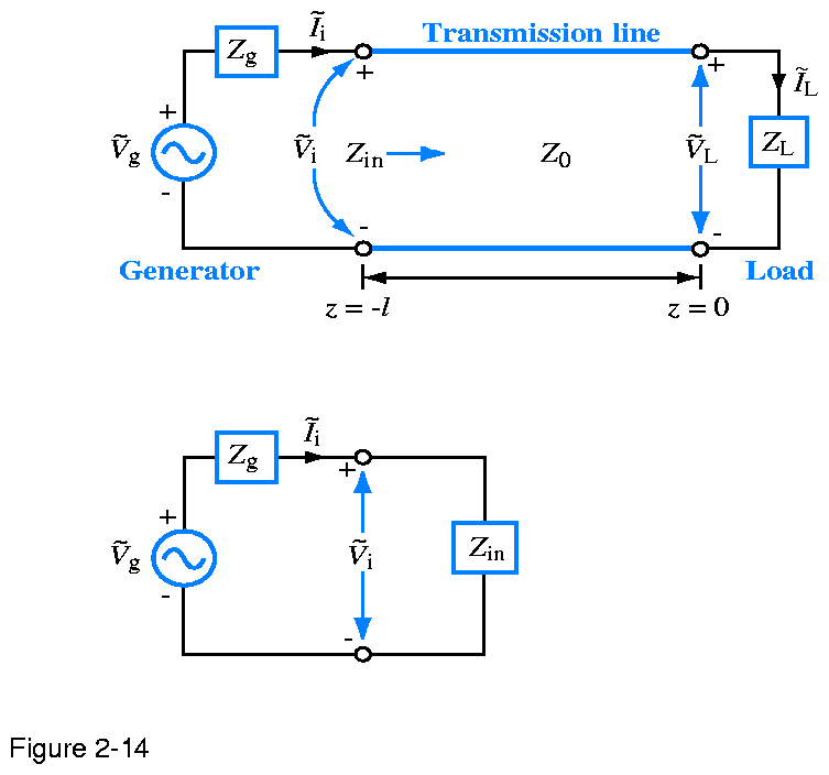
Figure 2.14: | At the generator end, the terminated transmission line
can be replaced with the input impedance of the line Zin.
|
|
|
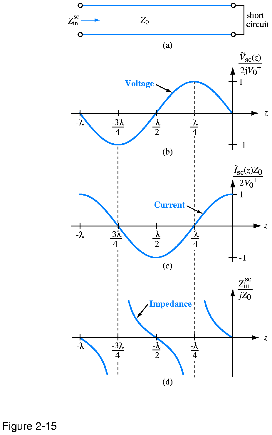
Figure 2.15: | Transmission line terminated in a short circuit: (a)
schematic representation, (b) normalized voltage on the line, (c)
normalized current, and (d) normalized input impedance.
|
|
|
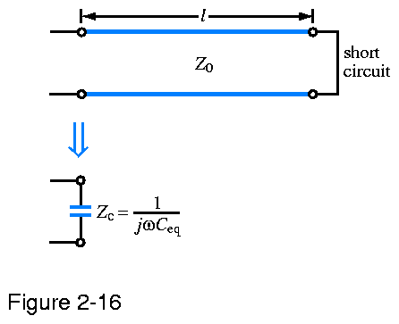
Figure 2.16: | Shorted lined as equivalent capacitor (Example 2-7).
|
|
|
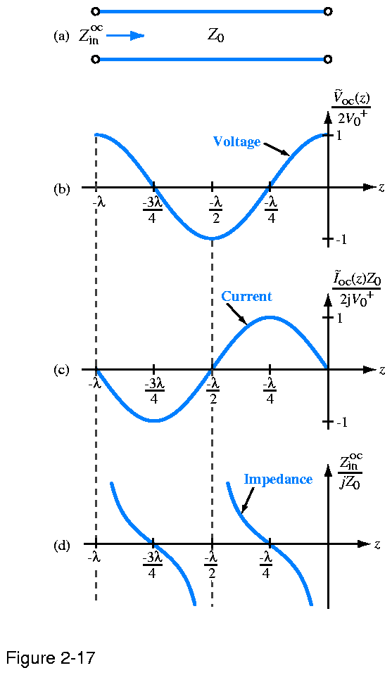
Figure 2.17: | Transmission line terminated in an open circuit: (a)
schematic representation, (b) normalized voltage on the line, (c)
normalized current, and (d) normalized input impedance.
|
|
|
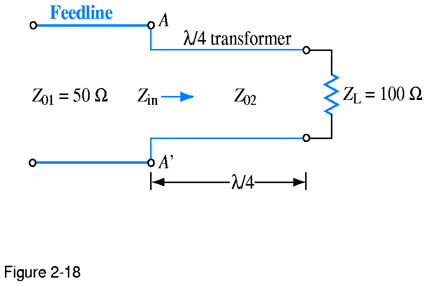
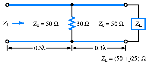
Figure 2.18: | Configuration for Example 2-9.
|
|
|
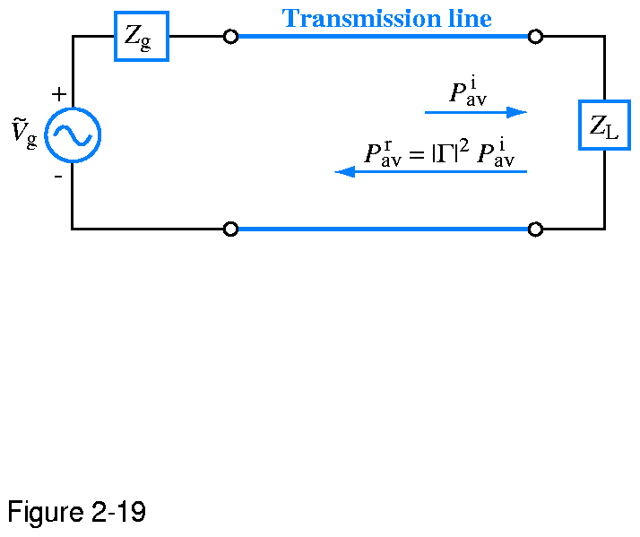
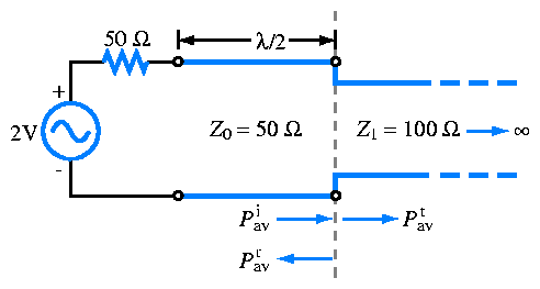
Figure 2.19: |
The time-average power reflected by a load connected to a
lossless transmission line is equal to the incident power multiplied by
by ||2.
|
|
|
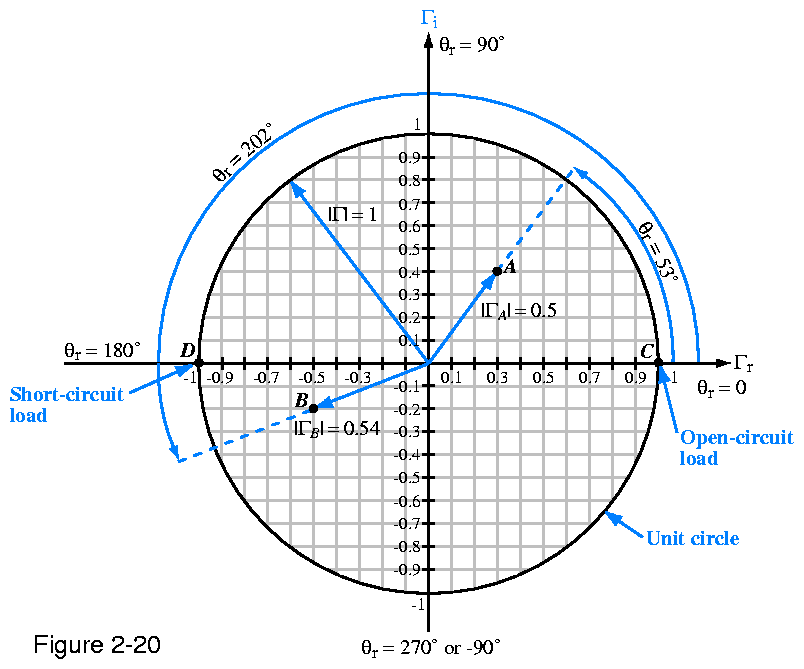
Figure 2.20: | The complex plane.
|
|
|
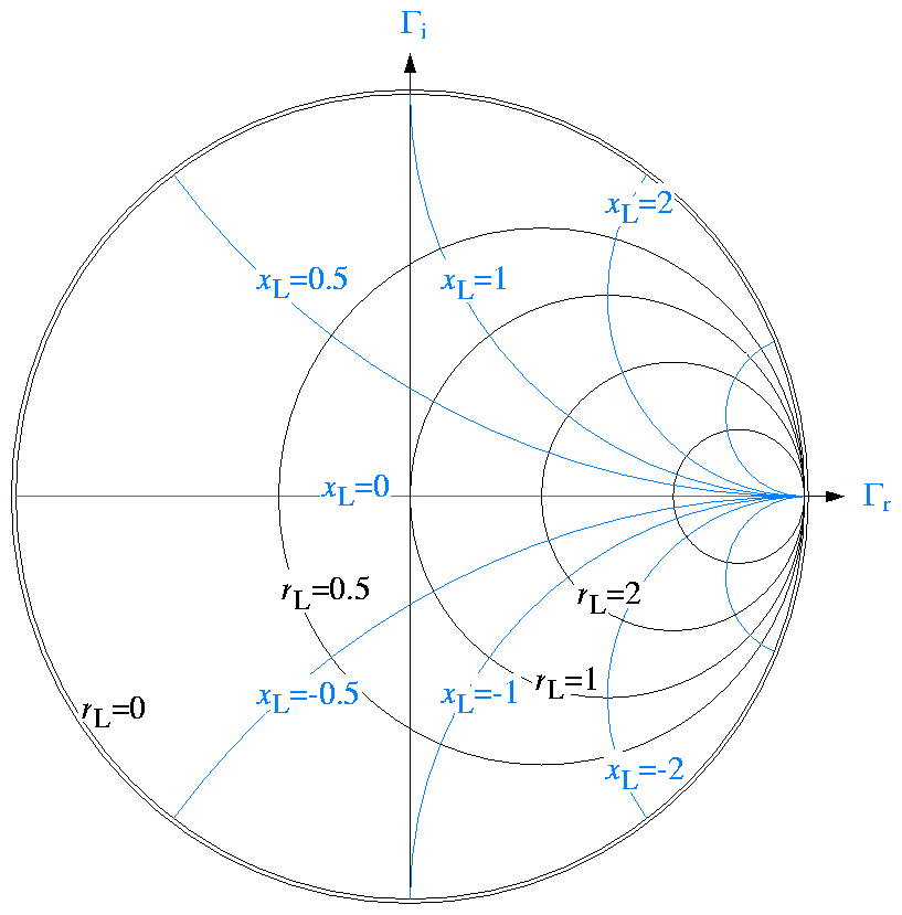
Figure 2.21: | Families of rL and xL circles within the domain.
|
|
|
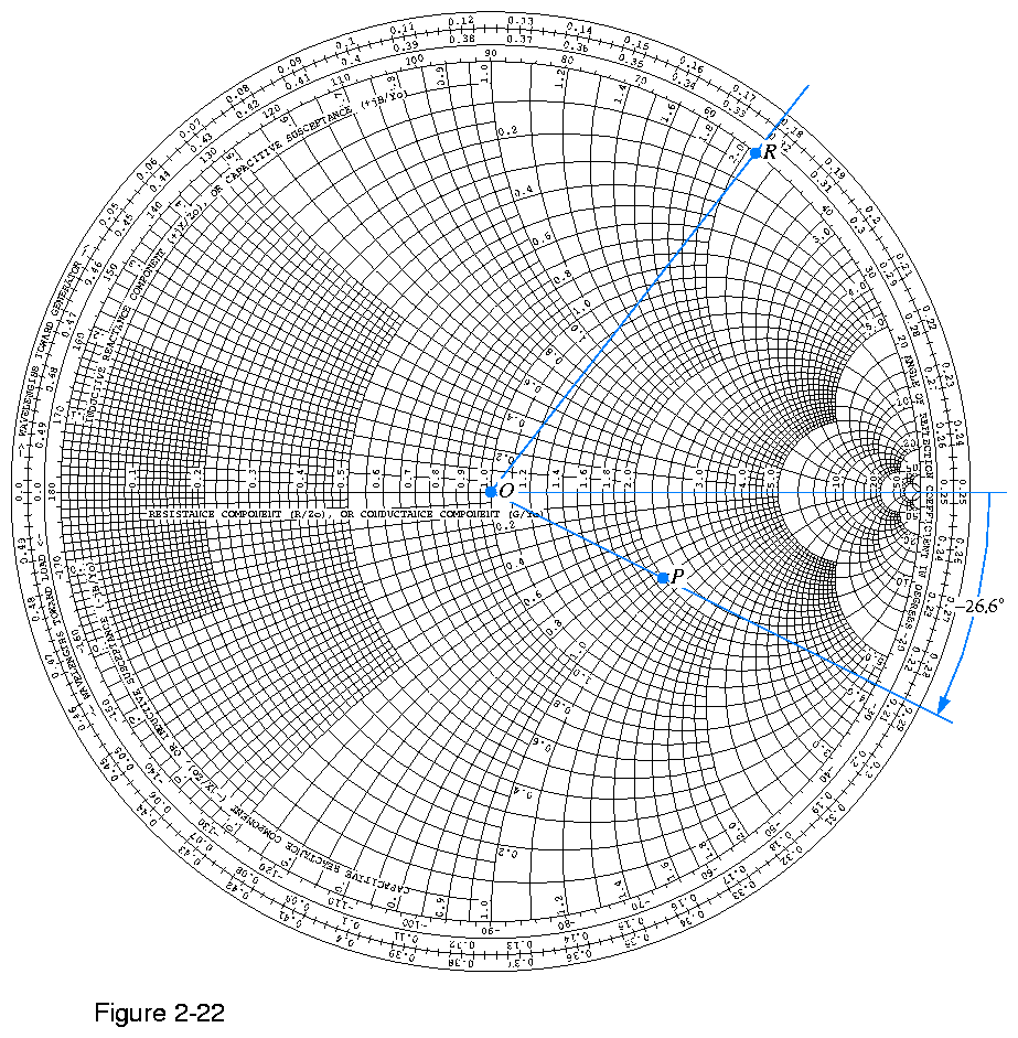
Figure
2.22: |
Point P represents a normalized load impedance ZL = 2 - j1.
The reflection coefficient has a magnitude || =OP/OR = 0.45 and
an angle  r = -26.6o. Point
R is an arbitrary point on the rL = 0 circle (which also is the
|| = 1 circle). r = -26.6o. Point
R is an arbitrary point on the rL = 0 circle (which also is the
|| = 1 circle).
|
|
|
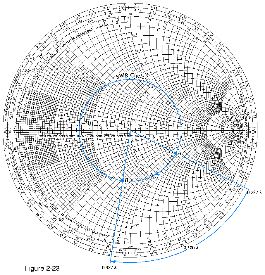
Figure 2.23: |
Point A represents a normalized load zL = 2 - j1 at
0.287  on the WTG scale.
Point B represents the line input at -.1 from the load.
At B, zin = 0.6-j0.66. on the WTG scale.
Point B represents the line input at -.1 from the load.
At B, zin = 0.6-j0.66.
|
|
|
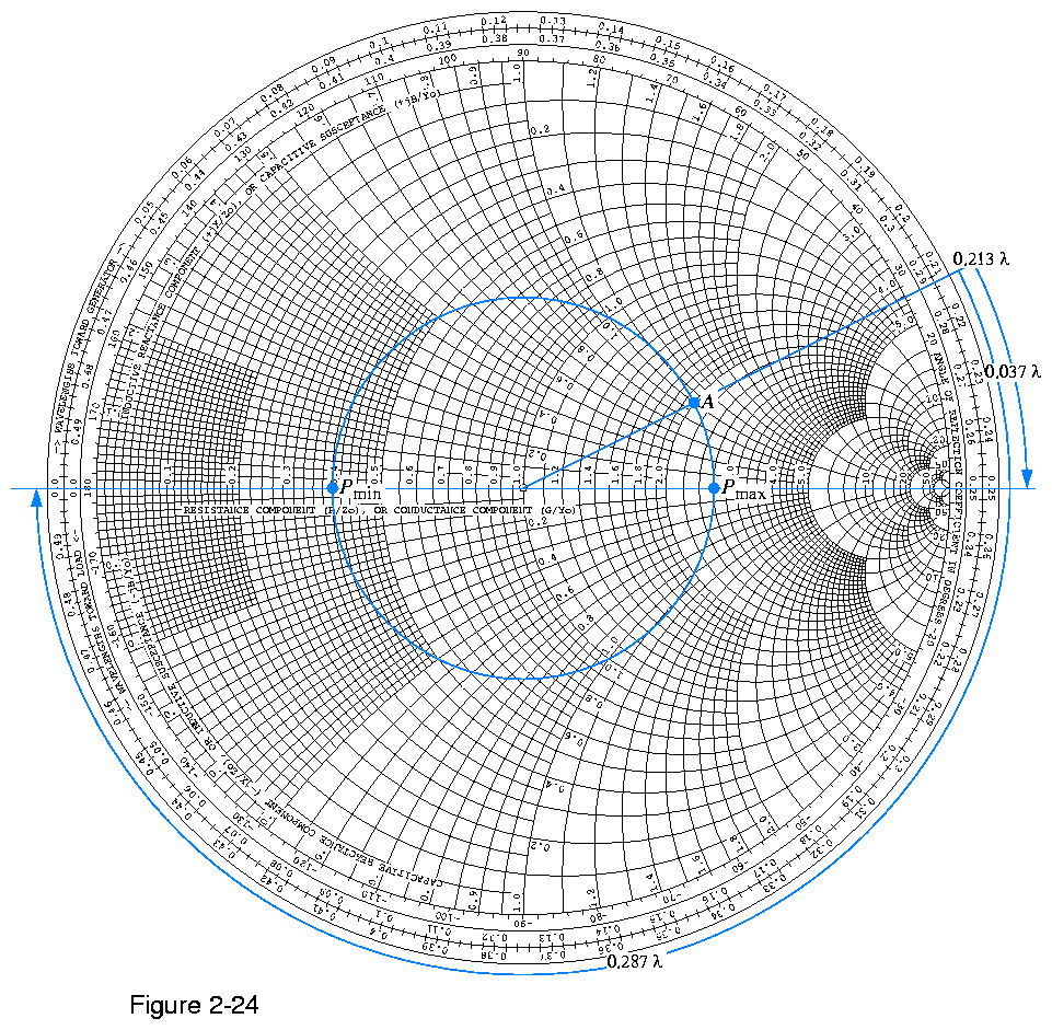
Figure 2.24: |
Point A represents a normalized load with zL = 2 + j1.
The standing wave ratio is S = 2.6 (at Pmax), the distance between the
load and the first voltage maximum is lmax = (0.25-0.213), and
the distance between the load and the first voltage minimum is lmin =
(0.037 + 0.25) = 0.287.
|
|
|
Figure 2.25: |
Point A represents a normalized load ZL = 0.6 + j1.4.
Its corresponding normalized admittance is yL = 0.25 - j0.6, and it is
at point B.
|
|
|
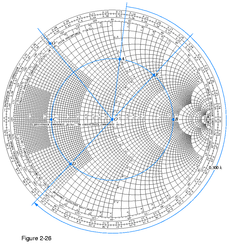
Figure 2.26: |
Solution for Example 2-10. Point A represents a
normalized load zL = 0.5 + j1 at 0.135 on the WTG scale. At
A, r = 83o and ||
= dA/d0'= 0A/00' = 0.62.
At B, the standing-wave ratio is S = 4.26. The distance from A to B gives lmax
= 0.115 and from A to C gives lmin = 0.365. Point D
represents the normalized input impedance zin = 0.28 - j0.40, and
point E represents the normalized input admittance yin = 1.15+j1.7.
|
|
|
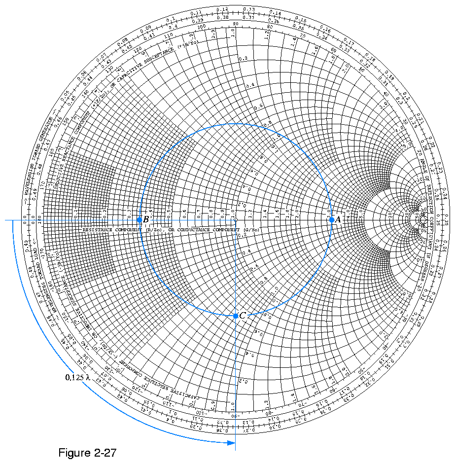
Figure 2.27: |
Solution for example 2-11. Point A denotes that S3,
point B represents the location of the voltage minimum, and point C
represents the load at 0.125 on the WTL scale from point B. At
C, zL= 0.6 - j0.8.
|
|
|
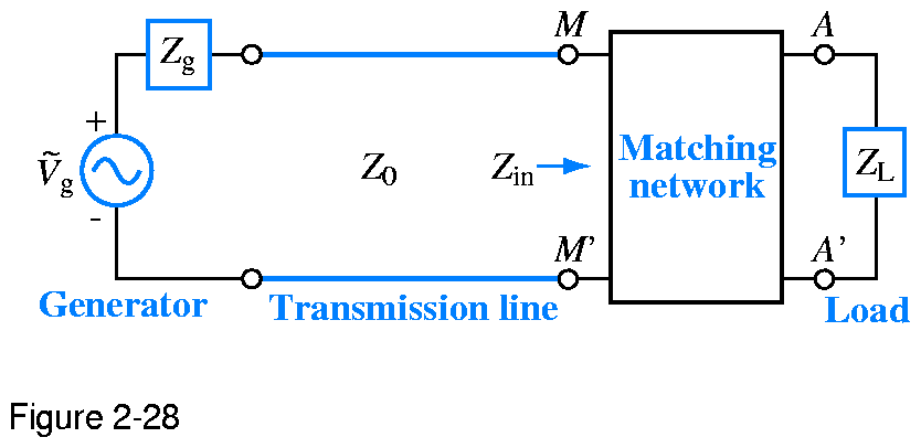
Figure 2.28: |
The function of a matching network is to transform the
load impedance ZL such that the input impedance Zin looking into the
network is equal to Z0 of the transmission line.
|
|
|
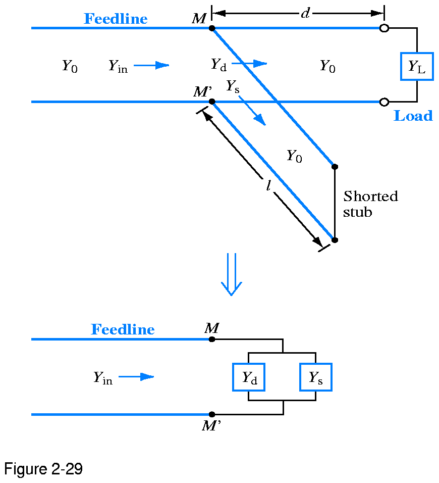
Figure 2.29: | Shorted-stub matching network.
|
|
|
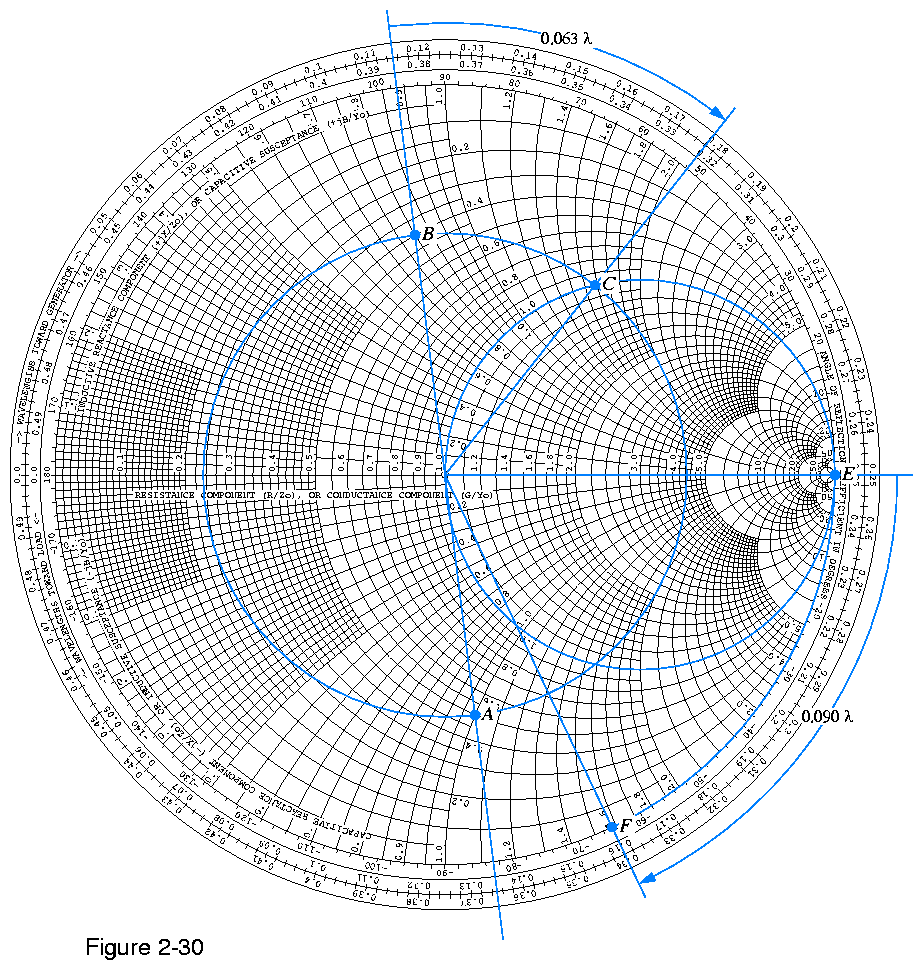
Figure 2.30: |
Solution for point C of Example 2-12. Point A is the
normalized load with zL = 0.5 - j1; point B is yL = 0.4 + j0.8. Point
C is the intersection of the SWR circle with the gL= 1 circle. The
distance from B to C is d1 = 0.063. The length of the shorted
stub (E to F) is l1= 0.09.
|
|
|
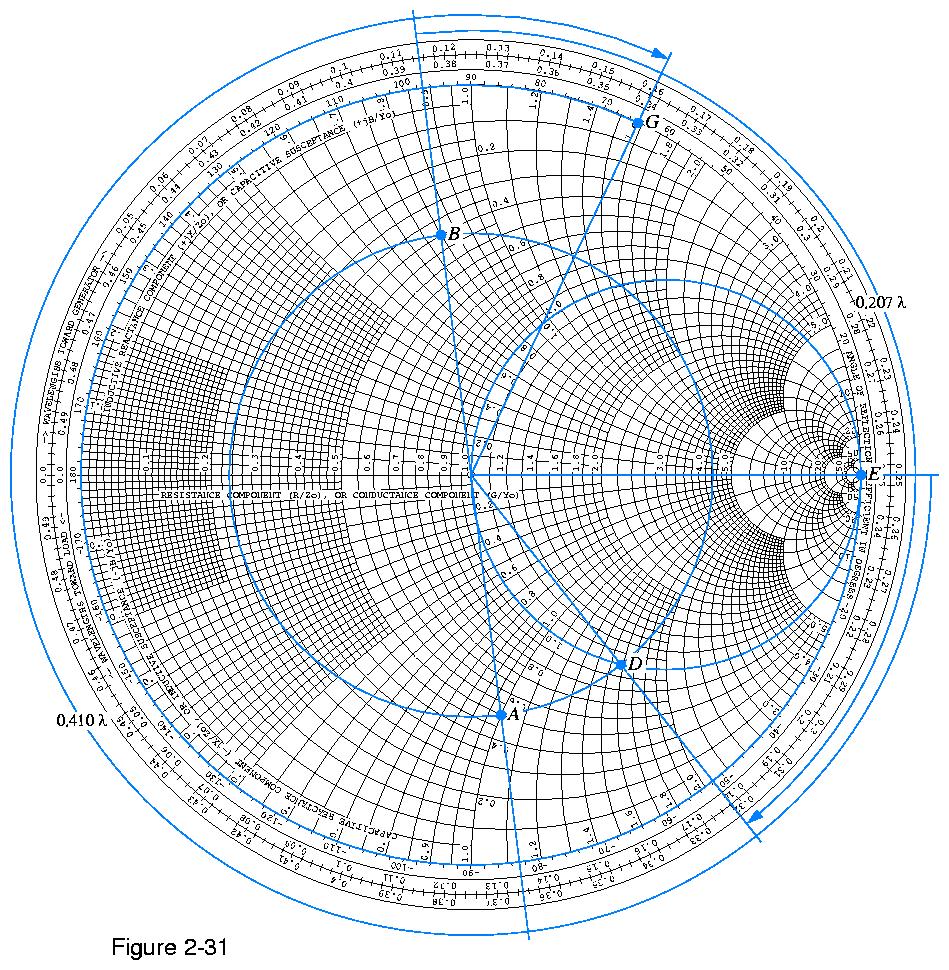
Figure 2.31: |
Solution for point D of Example 2-12. Point D is the
second point of intersection of the SWR circle and the yL= 1 circle.
The distance B to D gives d2= 0.207, and the distance E to G
gives l2= 0.410.
|
|
|
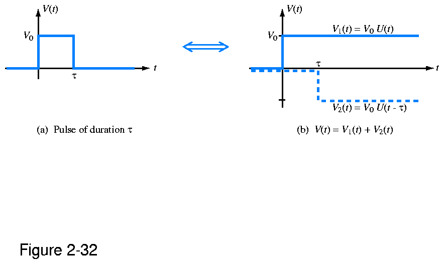
Figure 2.32: |
A rectangular pulse V(t) of duration  can be
represented as the sum of two step functions of opposite polarities
displaced by relative to each other. can be
represented as the sum of two step functions of opposite polarities
displaced by relative to each other.
|
|
|
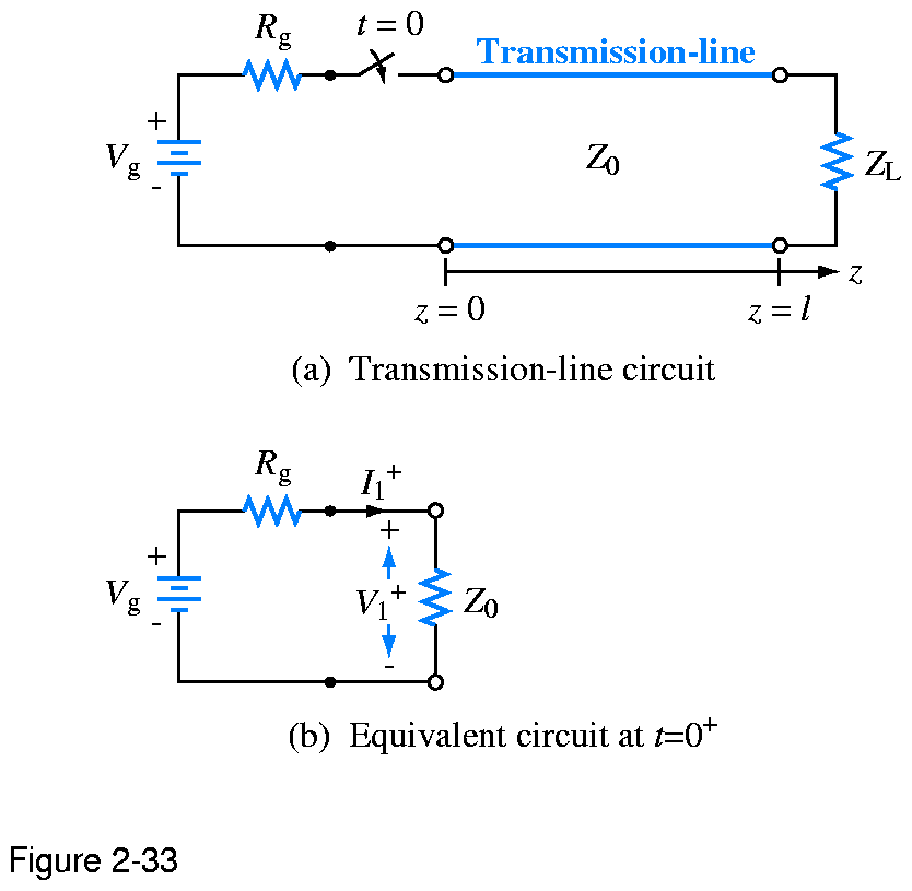
Figure 2.33: |
At t =0+, immediately after closing the switch in the
circuit in (a), the circuit can be represented by the equivalent
circuit on (b).
|
|
|
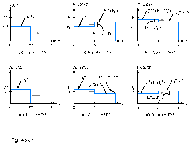
Figure 2.34: |
Voltage and current distributions on a lossless
transmission line at t=T/2, t=3T/2, and t=5T/2, due to a unit step
voltage applied to a circuit with Rg= 4Z0 and ZL= 2Z0. The
corresponding reflection coefficients are L= 1/3 and
g=3/5.
|
|
|
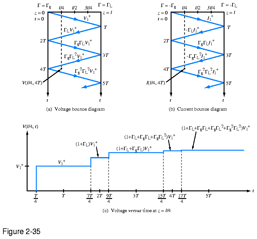
Figure 2.35: |
Bounce diagrams for (a) voltage and (b) current. In (c),
the voltage variation with time at z =l/4 for a circuit with g=
3/5 and L= 1/3 is deduced from the vertical dashed line at l/4
in (a).
|
|
|
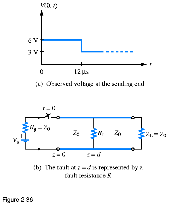
Figure 2.36: | Time-domain reflectometer of Example 2-13.
|
|
|
Figure 2.37: | Transmission-line model for Problem 2.4.
|
|
|
Figure 2.38: | Circuit for Problem 2.18.
|
|
|
Figure 2.39: | Circuit for Problem 2.23.
|
|
|
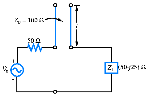
Figure 2.40: | Transmission-line arrangement for Problem 2.29.
|
|
|
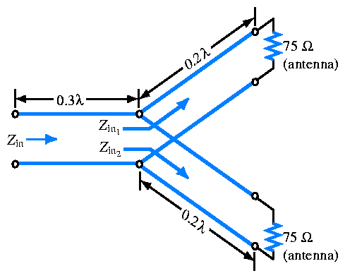
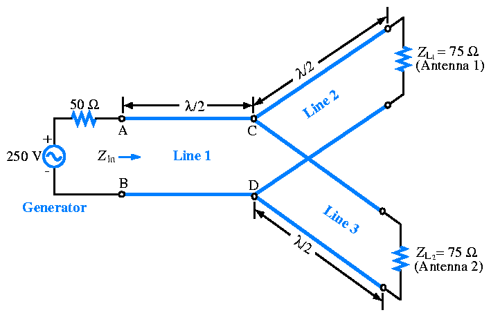
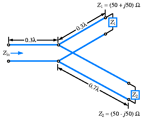
Figure 2.41: | Antenna configuration for Problem 2.32.
|
|
|
Figure 2.42: | Circuit for Problem 2.33.
|
|
|
Figure 2.43: | Circuit for Problem 2.45.
|
|
|
Figure 2.44: | Network for Problem 2.48.
|
|
|
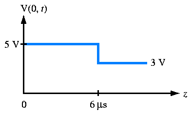
Figure 2.45: | Voltage waveform for Problems 2.53 and 2.54.
|
|
|
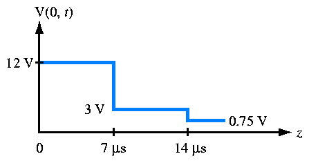
Figure 2.46: | Voltage waveform of Problem 2.53.
|