|


|
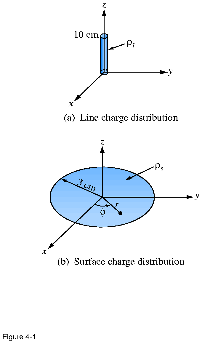
Figure 4.1: | Charge distributions for Examples 4-1 and 4-2.
|
|
|
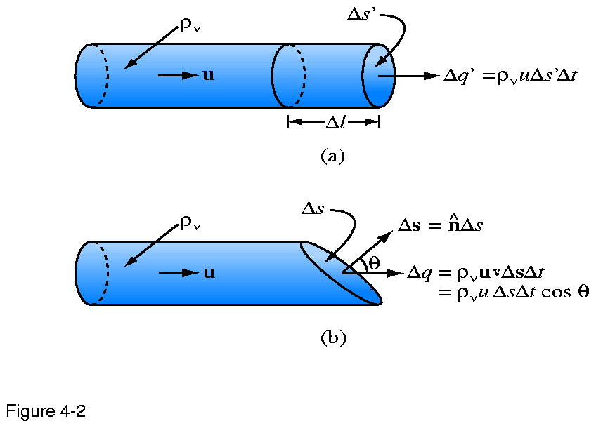
Figure 4.2: |
Charges with velocity u moving through a cross
section  s' in (a)
and s in (b). s' in (a)
and s in (b).
|
|
|
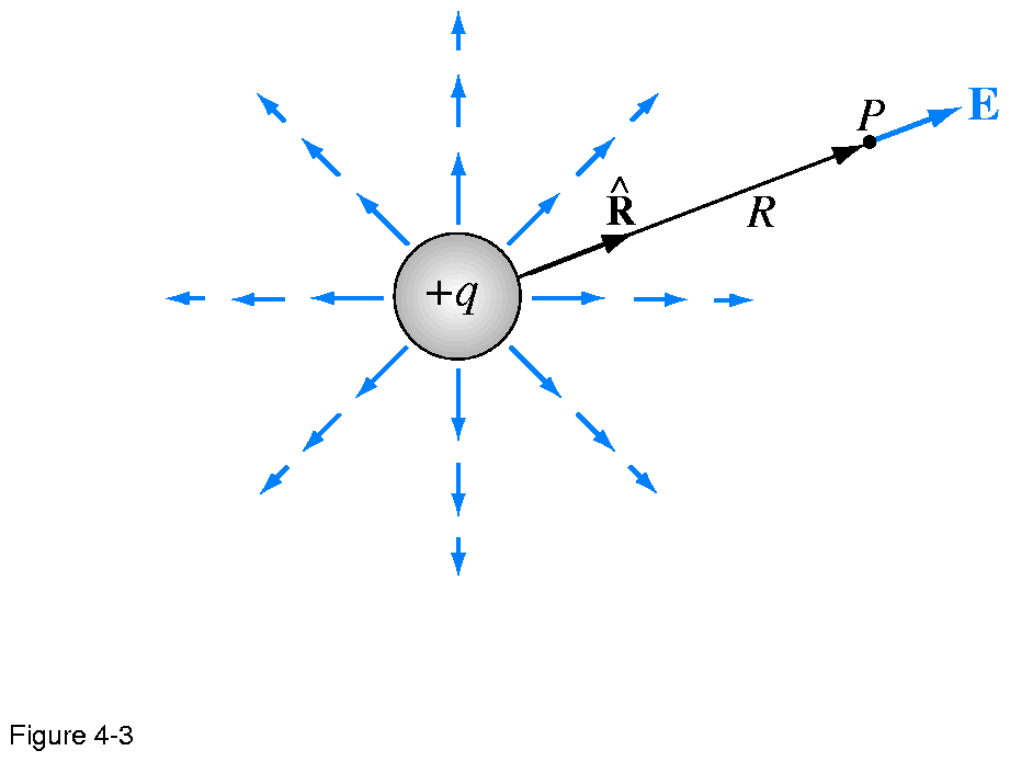
Figure 4.3: | Electric-field lines dues to a charge q.
|
|
|
Figure 4.4: |
The electric field E at P due to two charges is equal to
the vector sum of E1 and E2.
|
|
|
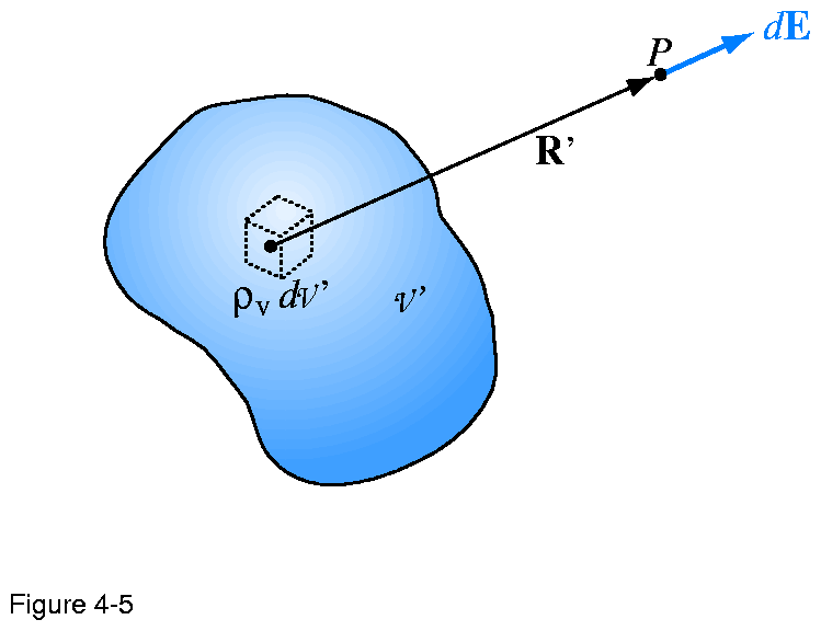
Figure 4.5: | Electric field due to a volume charge distribution.
|
|
|
Figure 4.6: |
Ring of charge with line density  l. (a) The field
dE1 due to infinitesimal segment 1 and (b) the fields dE1
and dE2 due to segments at diametrically opposite locations
(Example 4-4). l. (a) The field
dE1 due to infinitesimal segment 1 and (b) the fields dE1
and dE2 due to segments at diametrically opposite locations
(Example 4-4).
|
|
|
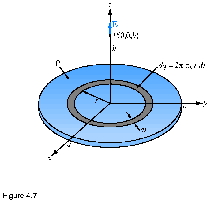
Figure 4.7: |
Circular disk of charge with surface charge density
s. The electric field at P(0,0,h) points along the z-direction
(Example 4-5).
|
|
|
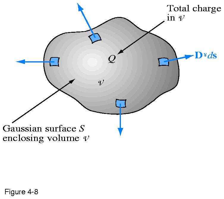
Figure 4.8: |
Gauss's law states that the outward flux of D
through a surface is proportional to the enclosed charge Q.
|
|
|
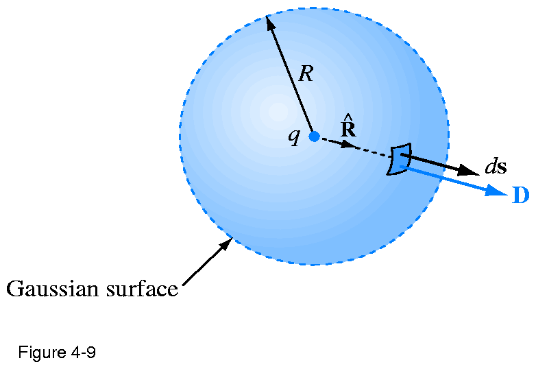
Figure 4.9: |
Electric field D due to point charge q.
|
|
|
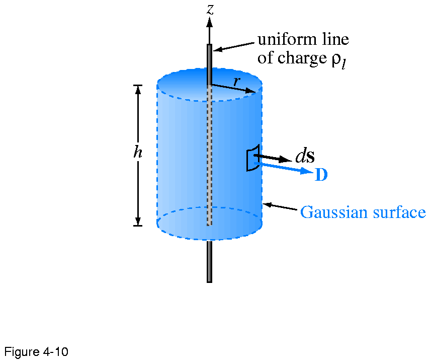
Figure 4.10: | Gaussian surface around an infinitely long line of charge
(Example 4-6).
|
|
|
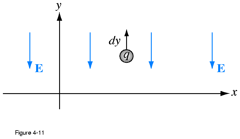
Figure 4.11: |
Work done in moving a charge q a distance dy against the
electric field E is dW = qE dy.
|
|
|
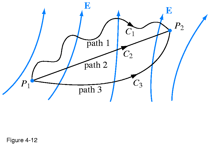
Figure 4.12: |
In electrostatics, the potential difference between P2
and P1 is the same irrespective of the path used for calculating the
line integral of the electric field between them.
|
|
|
Figure 4.13: |
Electric dipole with dipole moment p = q d
(Example 4-7).
|
|
|
Figure 4.14: |
Linear resistor of cross section A and length l connected
to a d-c voltage source V.
|
|
|
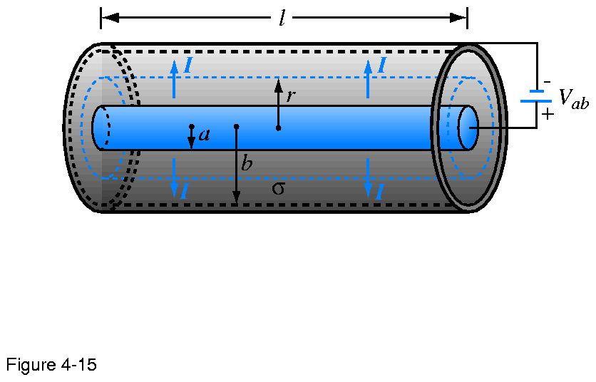
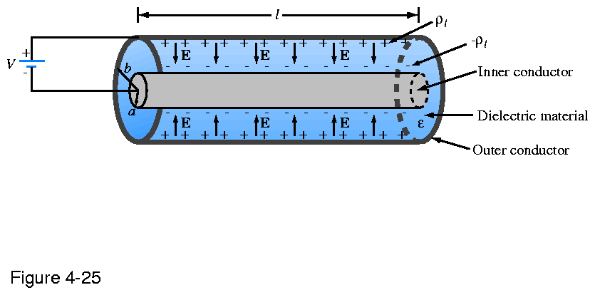
Figure 4.15: | Coaxial cable of Example 4-9.
|
|
|
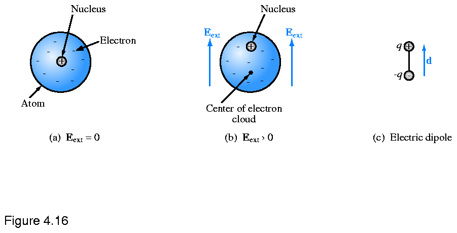
Figure 4.16: |
In the absence of an external electric field Eext,
the center of the electron cloud is co-located with the
center of the nucleus, but when a field is applied, the two centers are
separated by a distance d.
|
|
|
Figure 4.17: |
A dielectric medium polarized by an external electric
field Eext.
|
|
|
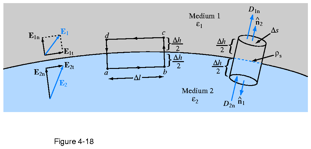
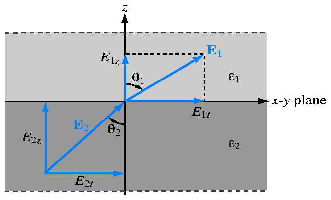
Figure 4.18: | Interface between two dielectric media.
|
|
|
Figure 4.19: |
Application of boundary conditions at the interface
between two dielectric media (Example 4-10).
|
|
|
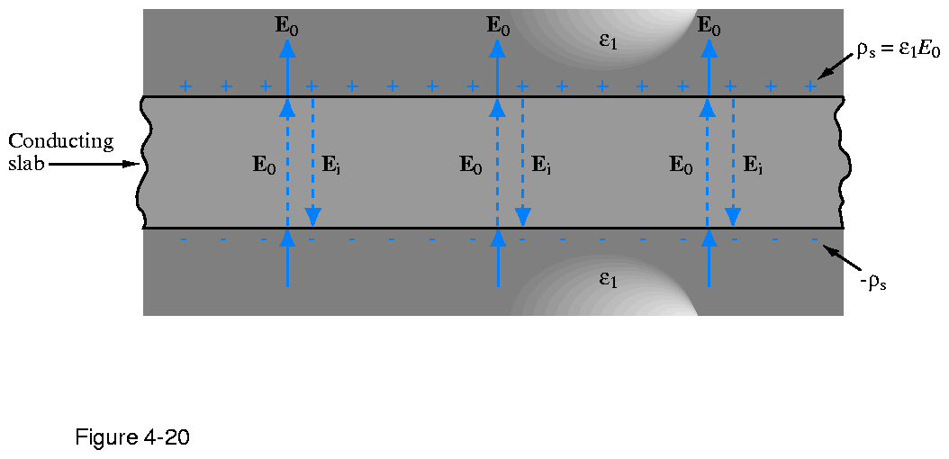
Figure 4.20: |
When a conducting slab is placed in an external electric
field E0, charges that accumulate on the conductor surfaces
induce an internal electric field Ei= -E0.
Consequently, the total field inside the conductor is zero.
|
|
|
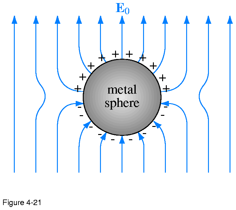
Figure 4.21: |
Metal sphere placed in an external electric field -E0.
|
|
|
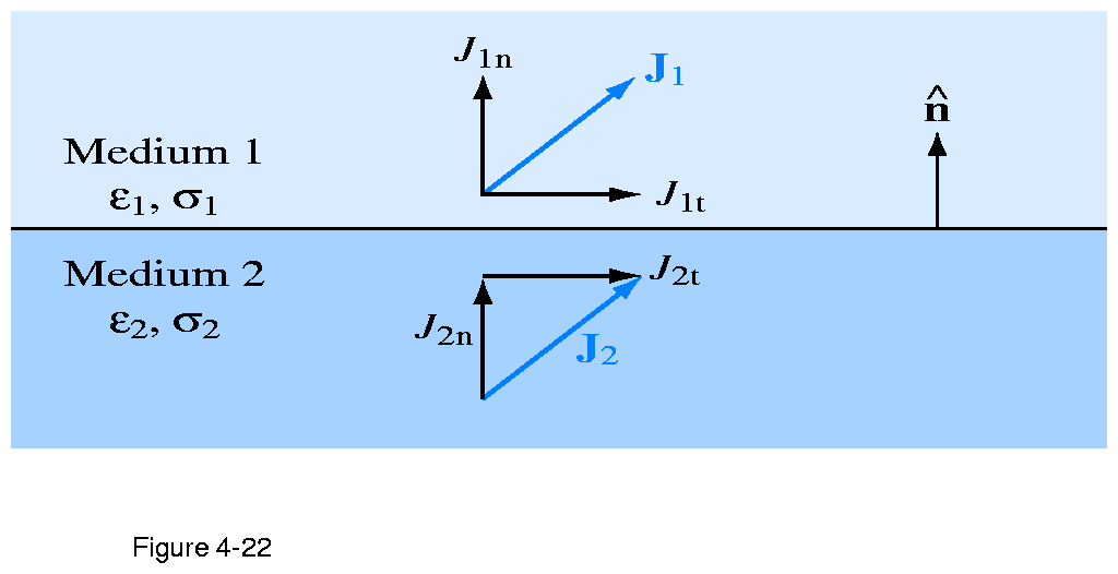
Figure 4.22: | Boundary between two conducting media.
|
|
|
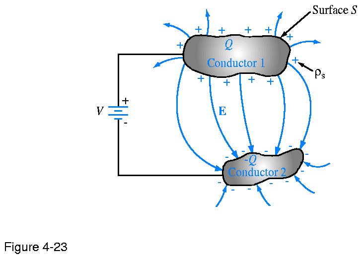
Figure 4.23: | A d-c voltage source connected to a capacitor composed of
two conducting bodies.
|
|
|
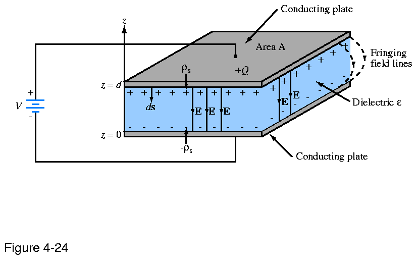
Figure 4.24: | A d-c voltage source connected to a parallel-plate
capacitor (Example 4-11).
|
|
|
Figure 4.25: |
Coaxial capacitor filled with insulating material of
permittivity  (Example 4-12). (Example 4-12).
|
|
|
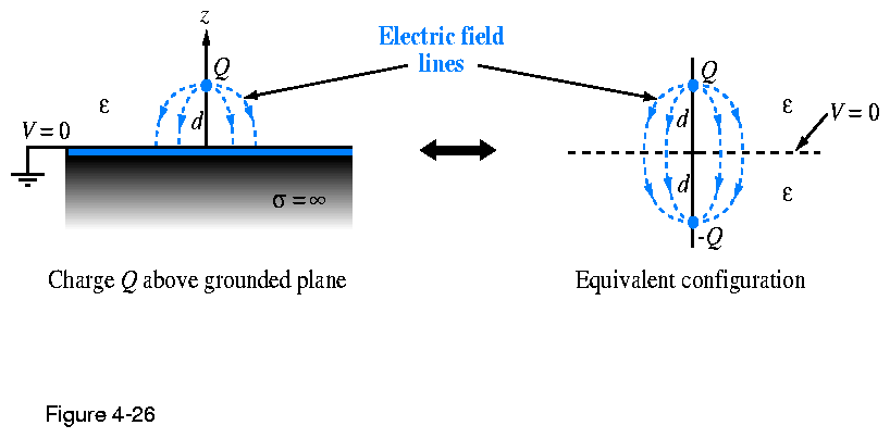
Figure 4.26: |
By image theory, a charge Q above a grounded perfectly
conducting plane is equivalent to Q and its image -Q with the ground
plane removed.
|
|
|
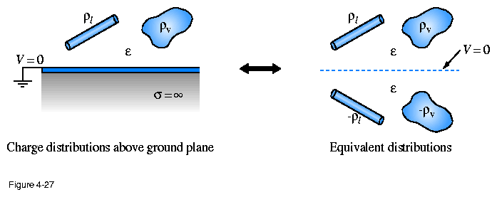
Figure 4.27: | Charge distributions above a conducting plane and their
image-method equivalents.
|
|
|
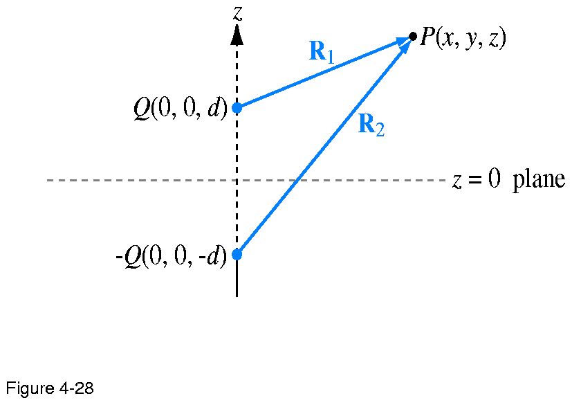
Figure 4.28: |
Application of the image method for finding E at
point P (Example 4-13).
|
|
|
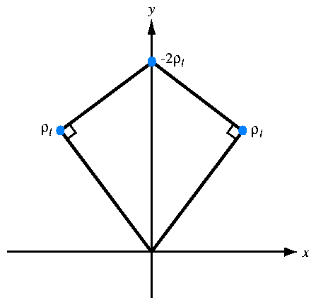
Figure 4.29: | Kite-shaped arrangement of line charges for Problem 4.17.
|
|
|
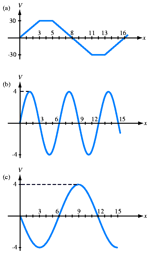
Figure 4.30: | Electric potential distributions of Problem 4.33.
|
|
|
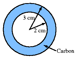
Figure 4.31: | Cross-section of hollow cylinder of Problem 4.41.
|
|
|
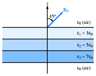
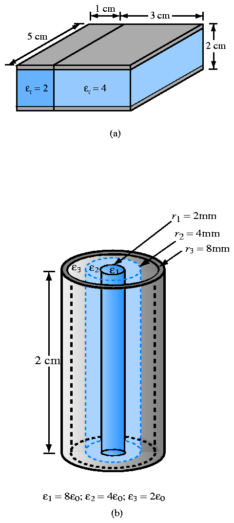
Figure 4.32: | Dielectric slabs in Problem 4.47.
|
|
|
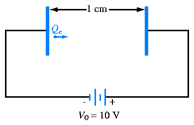
Figure 4.33: | Electron between charged plates of Problem 4.50.
|
|
|
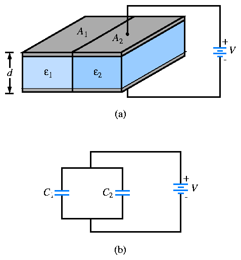
Figure 4.34: |
(a) Capacitor with parallel dielectric section, and (b)
equivalent circuit.
|
|
|
Figure 4.35: | Dielectric sections for Problems 4.53 and 4.55.
|
|
|
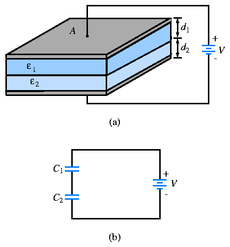
Figure 4.36: | (a) Capacitor with parallel dielectric layers, and (b)
equivalent circuit (Problem 4.54).
|
|
|
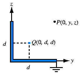
Figure 4.37: |
Charge Q next to two perpendicular, grounded, conducting
half-planes.
|
|
|
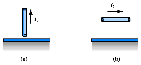
Figure 4.38: | Currents above a conducting plane (Problem 4.57).
|
|
|
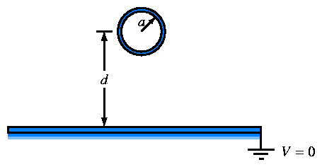
Figure 4.39: | Conducting cylinder above a conducting plane (Plane 4.58).
|